Products > Contact angle measuring systems + Micro scriber, Wafer contact angle, wafer stress measurement > SURFTENS HL automatic
Fully automatic contact angle meter for silicon wafers up to 12 inch
Get in touch >
SURFTENS HL automatic
Download PDF
Video
SURFTENS HL automatic
The professional solution for contact angle measurement in semiconductor technology
Features
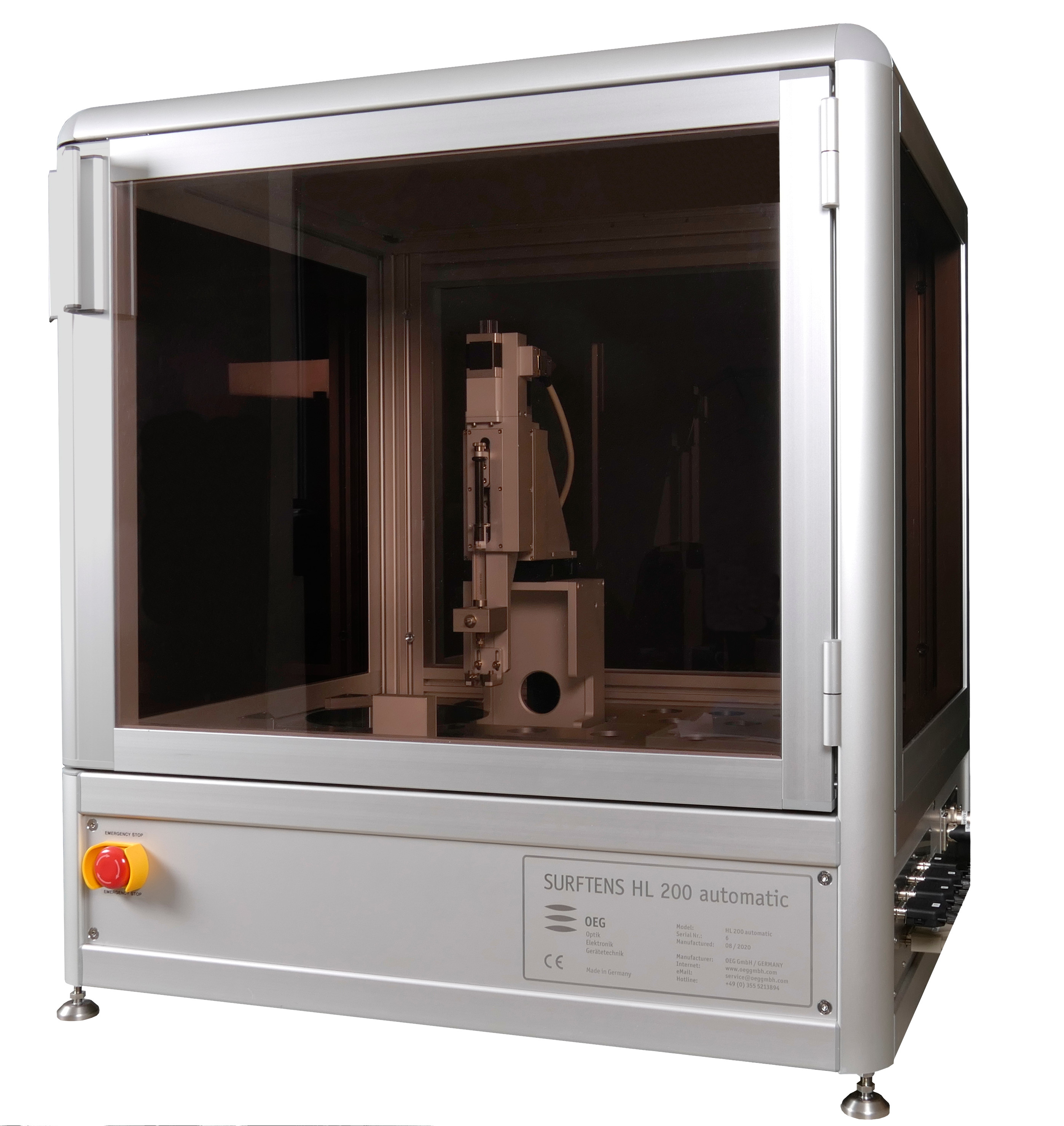
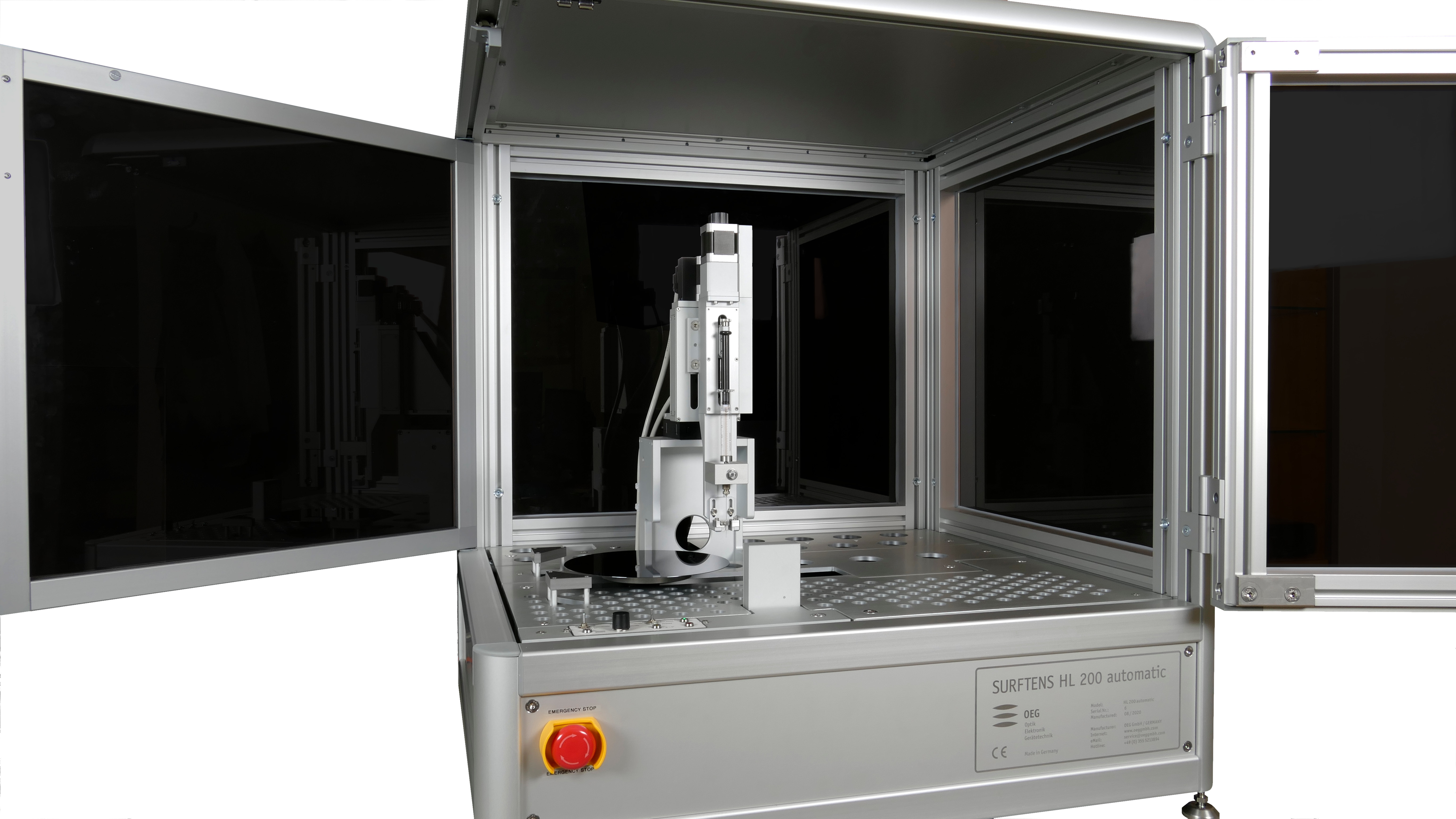
The contact angle measuring system SURFTENS HL automatic is designed for use in semiconductor industry and research, in particular for process control of wafer coating and in the photolithographic process.
It is characterized by the following features:
- fully automatic contact angle mappings
- space-saving construction
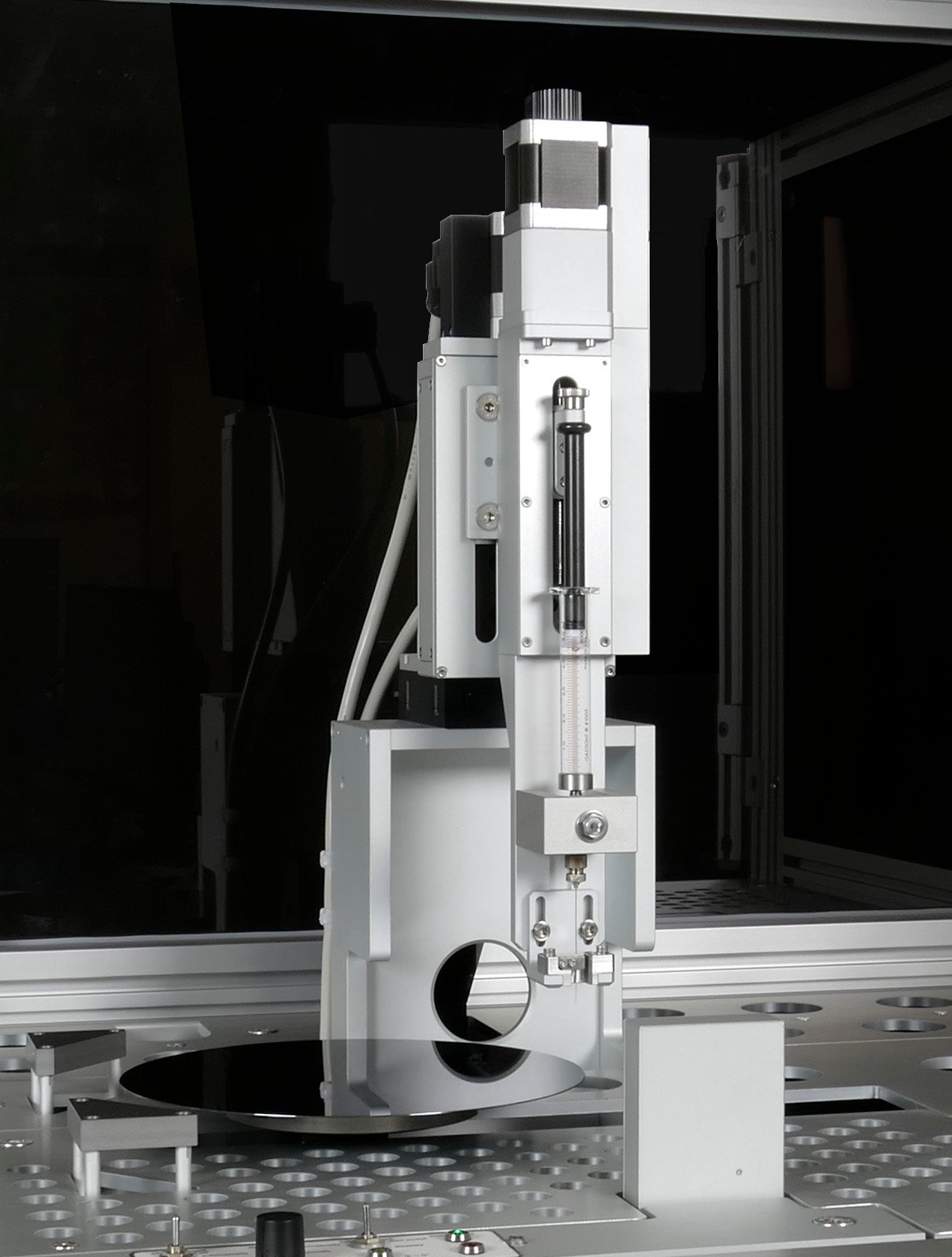
- motorized wafer table x/phi for automatic sample positioning
- motorized, automatic dosing unit
- automatic drop placement
- software controls fully automatic measuring sequence
- comfortable documentation of the measuring results in protocols and in the video images
Download PDF
Video