Industry & Application > Semiconductor Industry > FLATSCAN Waferstress Measuring System
Non contact automated measurement of warp, bow, slope and surface curvature with software module for calculation of thin film stress (wafer stress) of wafers and glass substrates.
Get in touch >
Download PDF
Product video
Description
Download PDF
Download product flyer
PDF FLATSCAN
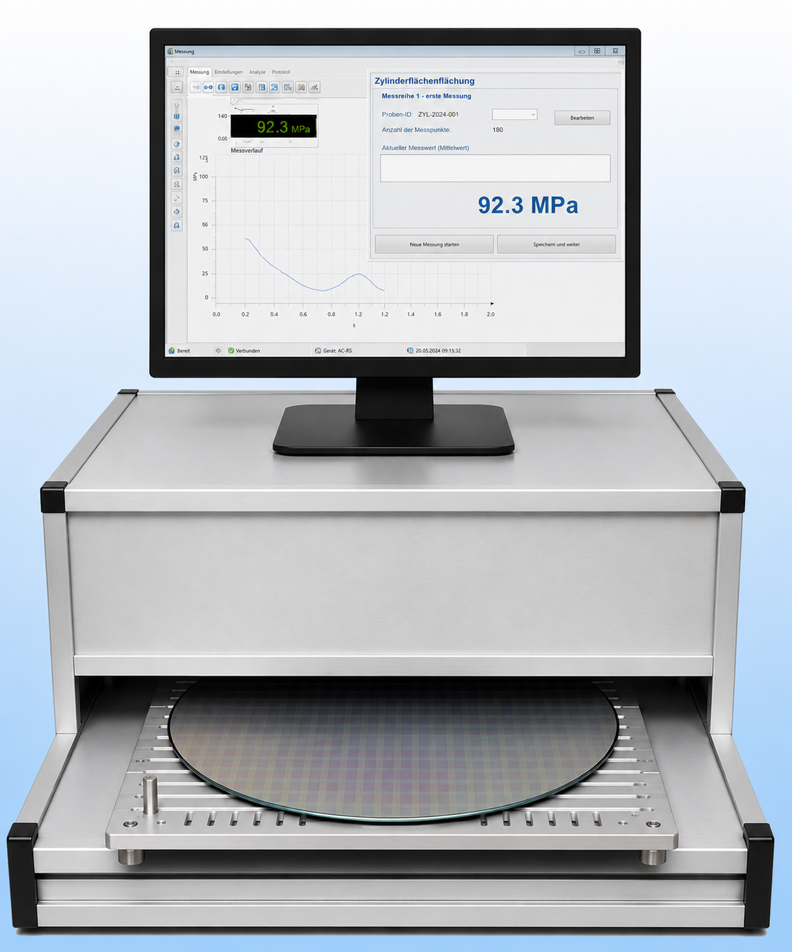
Product video
Description
Application
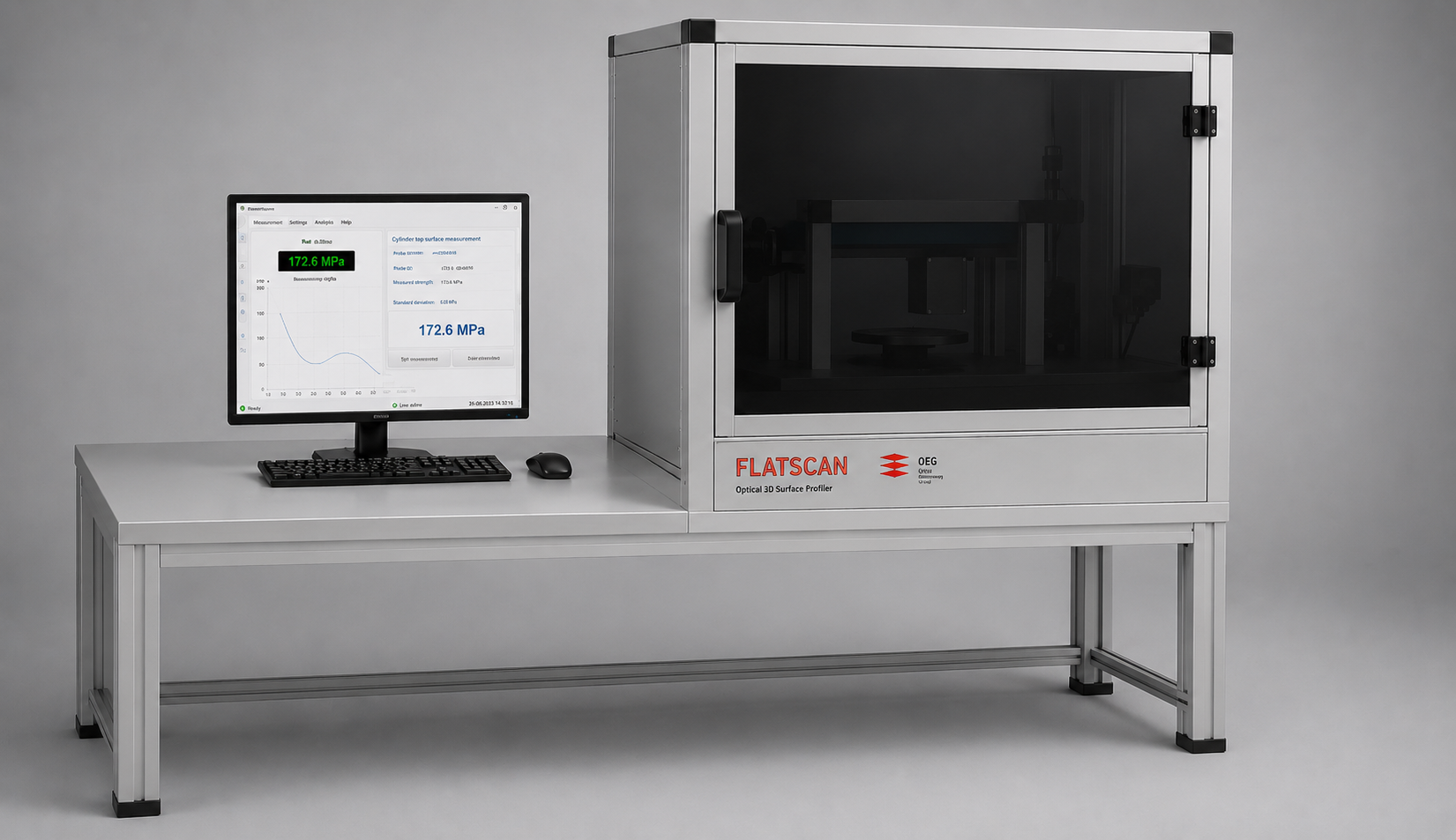
FLATSCAN serves for the contactless measurement of the surface profile and the calculation of thin film stress (waferstress) of all kinds of reflecting surfaces. This includes silicon wafers, mirrors, x-ray-mirrors (goebel-mirrors), metal surfaces or polished polymers. The optical measurement principle ensures a high measuring accuracy.
For applications in semiconductor technology the thin film stress in coatings can be calculated by the measured radii before and after coating.
Large measuring field
The standard measuring field diameter is 300mm.
High measuring accuracy
FLATSCAN is featured by a high measuring accuracy. The surface form reproducibility amounts to 100nm.
Large measuring range and working distance
The measuring range is the smallest measurable radius of curvature, which can be measured during one scan.
Scan length 100mm: Rmin 25m/ ±0,1m, Rmax ›10km/±1.5km
Scan length 200mm: Rmin 51m/±0.2m, Rmax ›20km/±3km
Scan length 300mm: Rmin 75m/±0.3m, Rmax ›30km/±4,5km
Different equipment types availabele
Depending on device type, single line scans or complete 3D scans can be accomplished.
The 3D-scans are assembled from numerous single line scans with automatic specimen positioning.
Software modul for calculation of thin film stress
For use in semiconductor technology and for all applications, where surface modifications (like coating or removal of coatings) are accomplished, the software is equipped with a module for the calculation of the thin film stress by the Fowkes theory.
The thin film stress is calculated from the mean radius of curvature before and after the coating process.
Technical Parameters
|
Parameter |
FLATSCAN |
|
Reproducibility surface curvature (P-V) |
≤ 100 nm** |
|
Resolution of optical measuring system |
0,1 arcsec |
|
Accuracy of optical measuring system |
1 arcsec |
|
Measuring speed |
10 mm…30 mm / sec |
|
Measuring field |
Standard: ø 300 mm |
|
Specimen thickness |
not limited |
|
Minimum Radius of curvature depending on scan length: |
|
|
100mm: Rmin 25m/ ±0,1m, Rmax ›10km/±1.5km |
|
|
200mm: Rmin 51m/±0.2m, Rmax ›20km/±3km |
|
|
300mm: Rmin 75m/±0.3m, Rmax ›30km/±4,5km |
|
|
|
|
|
free working distance |
not limited |
|
Measuring wavelength |
Standard: white light |
* standard equipment, can be adapted to othet demands
** Standard deviation at 50 measurements of the same scan with a standard specimen under standard measuring conditions